Computer architecture concerns the structure and properties of a computer system, as viewed from perspective of a software engineer while computer organisation is the same but as viewed from the perspective of a hardware engineer.
Microprocessor Organisation
Considerations:
- How large is your main store? (no. of words) x (no. of bits)
- PC should have enough bits to be able to refer to every word in the main store.
- How many programmatic instructions (the “function” the mnemonics refer to e.g.
CLEARorADD) do you want to provide to software engineers?- Remember that every processor architecture has a different type of assembly language (assembly language is very processor specific).
- The size of your opcode will dictate the number of instructions you can allow programmers to use. E.g. 3-bit opcode = 23 = 8 different instructions.
- Your subsystems will have to communicate – we do this with shared busses and three-state buffers.
- How many arithmetic instructions do you have? This directly affects the number of function selects your CU must have. E.g. Lets say your processor has 4 arithmetic instructions:
CLEAR,DEC1(decrement),INC1,ADD#somevalue. Then you will need 2 function selects from your CU to your ALU to specify which arithmetic instruction the ALU is executing.
Micro and Macro Instructions
Macro instructions are the set of mnemonics that each represent a specific instruction that your processor understands. These are assembled into opcodes that your CU can take to “know” which sequence of micro instructions to carry out.
Each micro instruction corresponds to a specific signal that your CU can assert (we call these control actions), and when carried out in the right sequence, the final result/effect is that of the macro instruction.
Clock cycles
The number of clocks a macro instruction takes in total is technically the time the CU takes to execute the instruction. Since the value of the data at the in our registers/certain outputs don’t change unless there is a clock supplied, we can further categorise macro instructions into the number of clock cycles or control steps needed.
What this implies is that certain micro instructions can be executed simultaneously, as long as their control actions are independent of one another (so their inputs/outputs don’t depend on each other and hence a clock/enable signal).
Representation of Instructions
We know that instructions have an opcode, may have an operand, and stored at a particular address in memory which the PC points to. The example below shows how instructions may look like in memory for a processor with a 32x8-bit Main Store, 5-bit PC, 3-bit opcode:
| Address | Mnemonic | Opcode Operand |
|---|---|---|
| 0 | CLEAR |
000 00000 |
| 1 | LOAD 5 |
110 00101 |
| 2 | ADD #8 |
010 01000 |
| … | – | – |
It is important to note that this is just an example; the key takeaway is to a better idea of how instructions are represented in memory.
❗❕ Remember that before and in between each instruction shown in the example above, there is an implicit fetch step (recall FDE cycle).
In RTL this would be:
[MAR] <- [PC][MDR] <- [MS(MAR)][IR] <- [MDR][PC] <- [PC] + 1
Note that the 4th step is actually a macro-step because the processor will have to have some mechanism of incrementing the PC, which can be done using the ALU or something else – it all depends on the processor architecture. What’s crucial is that you are aware of all these nuances and have them in mind when dealing with this topic.
Control Unit Design
Before we concern ourselves with the internal design of the CU, let’s analyse it with a black box approach which is to analyse it based on its requirements and how that affects what inputs and outputs the CU needs.
| Requirements of CU | Implication |
|---|---|
| Needs to operate at or near clock speed of microprocessor | Needs to have a clock input. |
| Needs to be aware of the state of bits in the CCR | Has to be connected to the CCR and its flags. |
| Needs to take opcode from the IR | Needs an input for Opcode. |
| Needs to translate opcode into appropriate sequence of processes to essentially execute opcode instructions. | Needs Enable, Clock, and Read/Write lines to all the components/subsystems to assert the sequence of signals to carry out the opcode. |
| Needs to specify which arithmetic operation to carry out. | Needs to have Function select lines leading to the ALU. The number of function selects = \(log_2(A)\), where \(A\) is the number of arithmetic operations. |
The CU executes micro instructions by asserting a sequence of enable and clock signals which have to abide by a timing diagram that depends on the particular macro instruction. Once we have this timing diagram for every opcode, we can form a truth table that models each macro instruction. This truth table helps us distinguish between control rounds/clock cycles needed and we can use it to help design our CU.
There are two main approaches to control unit design.
Hardwired / “Random Logic”. Design the CU as a combinatorial logic circuit, transforming its input signals into a set of output signals based on the truth table we mentioned above.
Microprogrammed. Each machine instruction is turned into a sequence of primitive microinstructions, which form a microprogram, stored in a ROM called the microprogram memory.
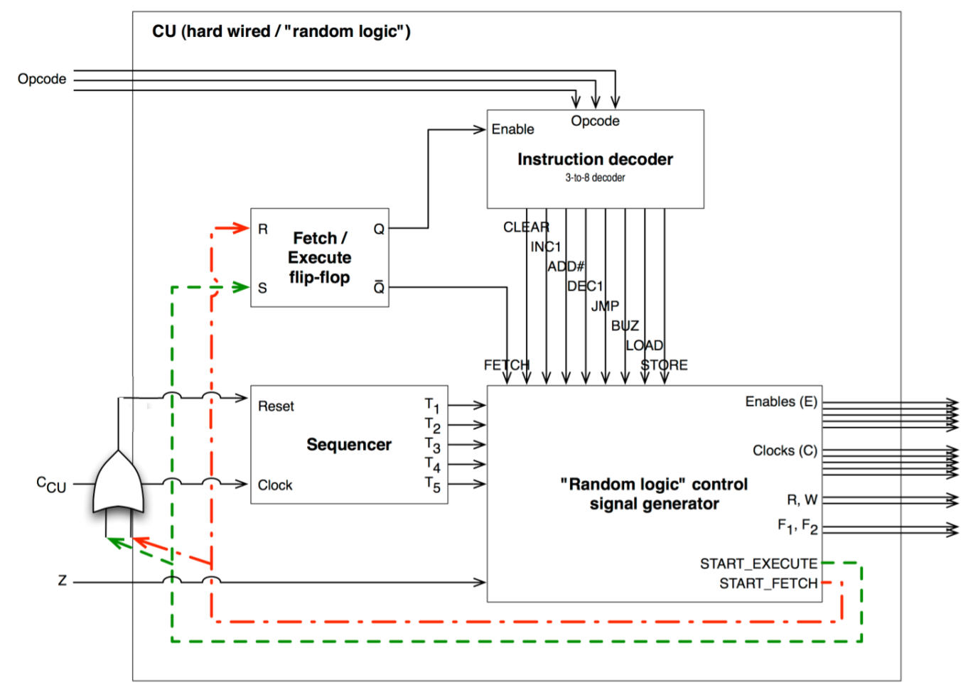
Hardwired CU
The dominant technique, since roughly 1980s, for implementing control units in RISC processors.
| Component | Function |
|---|---|
| Sequencer – takes clock input of our microprocessor | Regulates/aligns the operation of the combinatorial logic circuit in the CU with the control steps/rounds we have for each macro instruction. These regulated signals should ideally match the clock frequency. |
| Instruction Decoder | Depending on the opcode, send a signal to a certain path that corresponds to a particular macro instruction. |
| Fetch/Execute flip-flop | Depending on the START_FETCH and START_EXECUTE signals, the flip-flop ensures that the CPU is only ever fetching or carrying out an opcode instruction (XOR relationship). |
START_FETCH & START_EXECUTE |
When high, these two signals reset the sequencer so that it is in sync with the fetch/execute flip-flop’s signals (either the Enable signal to the opcode decoder or the fetch signal). |
Advantages. Fast (operates as fast as logic gates).
Disadvantages.
- Complex hardware makes it difficult to design and test – many interconnections.
- Inflexible as it is difficult to change the design if new instructions are added.
- Long design time.
Microprogrammed
The dominant technique for implementing CUs, peaking in 1970s, for CISC processors.
| Terminology | Description |
|---|---|
| Microprogram routine | Describes how to generate the CU outputs for one macro instruction. Made up of micro instructions and stored in microprogram memory (a ROM) |
| Microaddress | A location within microprogram memory |
| MicroPC | The CU’s internal program counter |
| MicroIR | Internal IR used to hold current micro instruction |
| Microinstruction | Holds the CU output values and other fields to control the microprogram flow. |
Advantages.
- Ease of design and implementation
- Flexibility of design allows families of processors to be built
- Simple hardware compared to hardwired implementations
- Microprogram memory can be reprogrammed for new instructions.
Disadvantages.
- Slower than hardwired implementations.
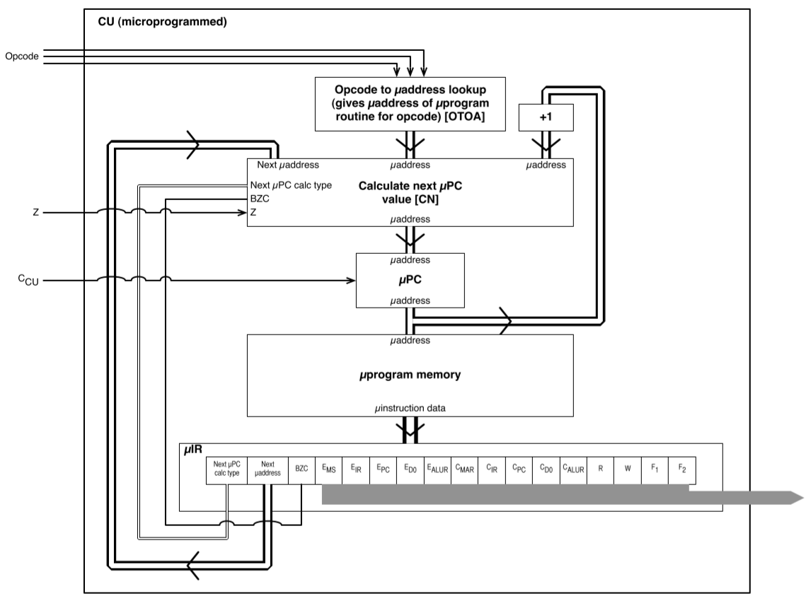
Standard operation description
- When the microPC is powered, it initialises to micro-address 0 which corresponds to the fetch micro-program.
- The micro-instruction register (microIR) receives microinstructions and this is where the CU output values are set to the values recorded in each micro-instruction of the program. Hence, the CU is able to generate the appropriate control signals, as the micro-program executes, which correspond to the macro fetch operation.
- After each microinstruction has generated CU outputs, the microPC is typically incremented to the next microinstruction by a +1 circuit, except for the last fetch microinstruction.
- At this point the processor’s IR has been populated with the next opcode and this is fed as opcode inputs into the CU.
- There is a component in the microIR we can call the “next microPC calc type” (I don’t think this is the actual name) that is set to make sure that the microPC is not incremented with the +1 circuit but instead is set to the output of an OTOA circuit (which is essentially a lookup table of opcodes to micro-program addresses).
- This enables the microPC to jump to the microaddress of the microprogram specified by the opcode and the CU can execute that microprogram based on the values set by the micro-instructions inside the program.
- When it is finally the last microinstruction, the “next microPC calc type” is set such that the microPC is now set to the microIR “next microaddress” field.
- Opcode microprograms use this facility/mechanism to set the microPC back to the fetch microprogram address.
CISC vs RISC
Complex Instruction Set Computers vs Reduced Instruction Set Computers.
Some history. Initially (1970s), the control store was much faster than main memory and therefore microprogrammed overhead was only 50% of execution time. As hardware got more advanced, both became faster but the control store lost its advantage and was about as fast as main memory. This led to microprogrammed overhead of over 80% of execution time. So even though processors were becoming more “capable” with a growing instruction set size, these were not actually enabling people to build better, more performant code.
Publishing results by Fairclough et al. in IEEE Micro (1982) supported this as it showed that certain groups of instructions are far more commonly used than others.
| Instruction Group | Frequency of Use |
|---|---|
Data movement (move, store, load) |
45.28% |
Program flow control (branch, call, return) |
28.73% |
Arithmetic (add, sub) |
10.75% |
Compare (cmp) |
5.92% |
Logical (and, or) |
3.91% |
| Shift | 2.93% |
| Bit manipulation | 2.05% |
| Miscellaneous | 0.44% |
Many people decided to take a fresh look at the situation and a paper by Patterson and Ditzel coined the two terms, RISC and CISC. They proposed a fresh start – a new approach to building our microprocessors (RISC) that did away with backward compatibility.
This sparked a split in industry, where ARM is the main proponent for RISC – their approach was to reduce the set of instructions but retain efficiency and synergy between control signal and control steps, sacrificing backwards compatibility.
Intel took a different approach and serves a market which wants backwards compatibility. They took a hybrid approach where the simplest and most commonly used instructions are executed by a RISC core and the more complex ones are microprogrammed (CISC). Performance is competitive and legacy software can still run.